Call Us

Call Us

Request quote

Need Estimate?

Request a quote
SPATIAL WAFERMAP
SPATIAL WAFERMAP

SPATIAL WAFERMAP

MOQ : 1 Unit

SPATIAL WAFERMAP Specification

  • Power Source
  • External Adapter
  • Input
  • Wafer map data files
  • Operating Temperature
  • 10C to 40C
  • IP Rating
  • IP20
  • Features
  • Real-time mapping, defect detection, data export
  • Power Supply
  • External AC/DC Adapter
  • Components
  • Sensing module, display, interface board
  • Processor Speed
  • 1.6 GHz
  • Interface
  • USB, LAN, RS-232
  • Display Type
  • LCD touchscreen
  • Response Time
  • <2 s
  • Output
  • Graphical spatial wafer map
  • Usage
  • Wafer inspection and analysis
  • Sensors Specification
  • High accuracy position sensors
  • Resolution
  • 1280 x 800 pixels
  • Product Type
  • Wafer Map Analyzer
  • Application
  • Semiconductor manufacturing, process control, quality assurance
  • Rated Voltage
  • 5V DC
  • Supply Voltage
  • 100-240V AC
  • Size
  • Portable desktop module
  • Dimension (L*W*H)
  • 320 mm x 210 mm x 80 mm
  • Function
  • Semiconductor wafer mapping and visualization
  • Color
  • White and Blue
  • Weight
  • 2.5 kg
  • Capacity
  • Supports up to 12-inch wafers
  • Current Rating
  • 0.5A
  • Thickness
  • Standard: 10 mm
  • Frequency
  • 50/60 Hz
  • Alarm System
  • Audio and on-screen alerts
  • Software Compatibility
  • Windows 7/8/10, Linux Support
  • Installation
  • Standalone or integrated with fab MES
  • Language Support
  • Multilingual UI (English, Japanese, Chinese)
  • Humidity Range
  • 20%-80% RH (non-condensing)
  • Network Connectivity
  • Ethernet 10/100/1000 Mbps
  • Calibration
  • Factory calibrated, user re-calibration possible

  • Data Storage Capacity
  • Up to 100,000 records
  • Power Consumption
  • Max 15W
  • User Access Control
  • Multi-level password protection
  • Maintenance
  • Tool-free sensor replacement
  • Compliance
  • CE, RoHS, ISO9001
  • Data Export Format
  • CSV, PDF, proprietary image
  • Map Visualization Modes
  • 2D, Heatmap, Cluster analysis


About SPATIAL WAFERMAP


The SPATIAL WAFERMAP is a celebrated, hot-selling semiconductor wafer mapping solution, renowned for its brilliant features and top-rated user-friendly interface. Engineered for optimum performance, it supports Windows and Linux, offers real-time defect detection, and visualizes wafer data through versatile 2D, heatmap, and cluster analysis modes. Favorable reviews underscore its robust data export options (CSV, PDF, proprietary images) and extensive compatibility, including Ethernet connectivity, multilingual support, and MES integration. Reliable calibration, rigorous compliance standards, and tool-free maintenance make it a top choice for semiconductor manufacturing and process control environments.

Versatile Application and Superior Usage

SPATIAL WAFERMAP is ideal for semiconductor manufacturing, process control, and quality assurance. As a portable desktop module, it supports various wafer sizes up to 12 inches and efficiently handles input wafer map data files. Use it for advanced inspection and spatial visualization in labs or fabs, providing crucial analysis for defect detection and yield optimization. Its adaptability and user-recalibration ensure precision across diverse application scenarios, making it essential for modern semiconductor environments.


Packaging, Samples, and Export Market Coverage

Each SPATIAL WAFERMAP unit is securely packaged for safe delivery and arrives promptly after order completion. Samples are available by request, allowing evaluation before full purchase. With a competitive sale price and careful logistics, this product is delivered to key export markets, especially in South Korea and Asia-Pacific. Dedicated export services ensure the product reaches your facility intact and on time, supporting your production continuity.


FAQ's of SPATIAL WAFERMAP:


Q: How can I use SPATIAL WAFERMAP with my current manufacturing systems?

A: SPATIAL WAFERMAP seamlessly integrates with your fab MES, supporting standalone or networked operation via Ethernet, USB, and RS-232 interfaces for efficient data transfer and automation.

Q: What are the main benefits of using SPATIAL WAFERMAP in process control?

A: It offers real-time defect detection, advanced visualization (2D, heatmap, cluster analysis), and precise mapping, enabling process optimization and higher manufacturing yield through timely, reliable data.

Q: Where is SPATIAL WAFERMAP primarily used?

A: This tool is primarily deployed in semiconductor manufacturing plants, research labs, and quality assurance departments to support wafer inspection, process control, and data-driven analysis.

Q: What is the process for recalibrating the device?

A: Users can perform re-calibration using the intuitive LCD touchscreen interface, ensuring ongoing accuracy without specialized tools. Factory calibration is provided, and user-guided adjustment is supported as needed.

Q: How does SPATIAL WAFERMAP handle data export and storage?

A: The device can export data in CSV, PDF, and proprietary image formats. It supports storing up to 100,000 records, with quick access and real-time data export for efficient documentation and reporting.

Tell us about your requirement
product

Price:

Quantity
Select Unit

  • 50
  • 100
  • 200
  • 250
  • 500
  • 1000+
Additional detail
Mobile number

Email

More Products in Electronics Category
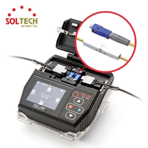
Economical - High Performance Core Alignment Splicer Mini 5C

Economical - High Performance Core Alignment Splicer Mini 5C

Minimum Order Quantity : 100 Units

Features : Economical, High performance, Mini size, Fast splice time

Color : Black & Orange

Application : FTTH, Telecommunication, Broadband

Size : Mini

Function : Optical fiber fusion splicing

InforTab (ESL Electronic Shelf Labels Retail Marketing Smart Retail Operation Hospital)

InforTab (ESL Electronic Shelf Labels Retail Marketing Smart Retail Operation Hospital)

Minimum Order Quantity : 1 Unit

Features : Wireless update, tamper detection, barcode/QR code display, multicolor labels, centralized management

Color : White with black, red, or yellow eink display

Application : Retail shelves, price automation, smart retail, hospitals

Size : 1.54, 2.13, 2.9, 3.7, and 4.2 (diagonal sizes available)

Function : Digital pricing, product information display, automated price updates, inventory management, order processing, system integration

ANBAC Laptop Privacy Screen Shield

ANBAC Laptop Privacy Screen Shield

Minimum Order Quantity : 100 Units

Features : Antiscratch, antiglare, blue light reduction, easy installation, removable, reusable

Color : Black

Application : Laptops, Notebooks, Business, Education, Personal Use

Size : Available for 13.3 inch, 14 inch, 15.6 inch, 17.3 inch laptops

Function : Privacy protection for laptop screen, antiglare, antispy, screen filter

0.6/1kV HiRaCS Halogen-Free Cable(HiRaCS HFCO/AAAC)

0.6/1kV HiRaCS Halogen-Free Cable(HiRaCS HFCO/AAAC)

Minimum Order Quantity : 1000

Features : High Quality

Color : as shown in the image

Application : Electrical & Electronics

Size : Standard

Function : Electrical & Electronics Equipment


Back to top